Why Google's 8th Gen TPUs Matter
Google's split TPU architecture for training and inference, and why it matters for frontier AI.
For the past few years, the narrative surrounding AI hardware has been pretty straightforward: NVIDIA is the undisputed king 👑.
Looking at raw, per-chip specifications, NVIDIA’s Hopper, Blackwell, and upcoming Rubin chips generally crush the competition. But recently, frontier labs have been hitting a wall, and it’s fundamentally changing how we should evaluate AI compute.
Setting aside supply chain bottlenecks (HBM scarcity, maxed-out manufacturing capacity) and energy worries, labs training trillion parameter models are no longer constrained purely by the speed of an individual chip (measured in FLOPs). Rather, they’re limited by memory bandwidth, network latency, and the cluster itself.
To address the diverging “demand profiles” of the Agentic era, Google recently announced their 8th generation of TPUs. Moving away from their “one-size-fits-all” approach, they split their chip architecture for two distinct workloads: the 8t (for training) and 8i (for inference).
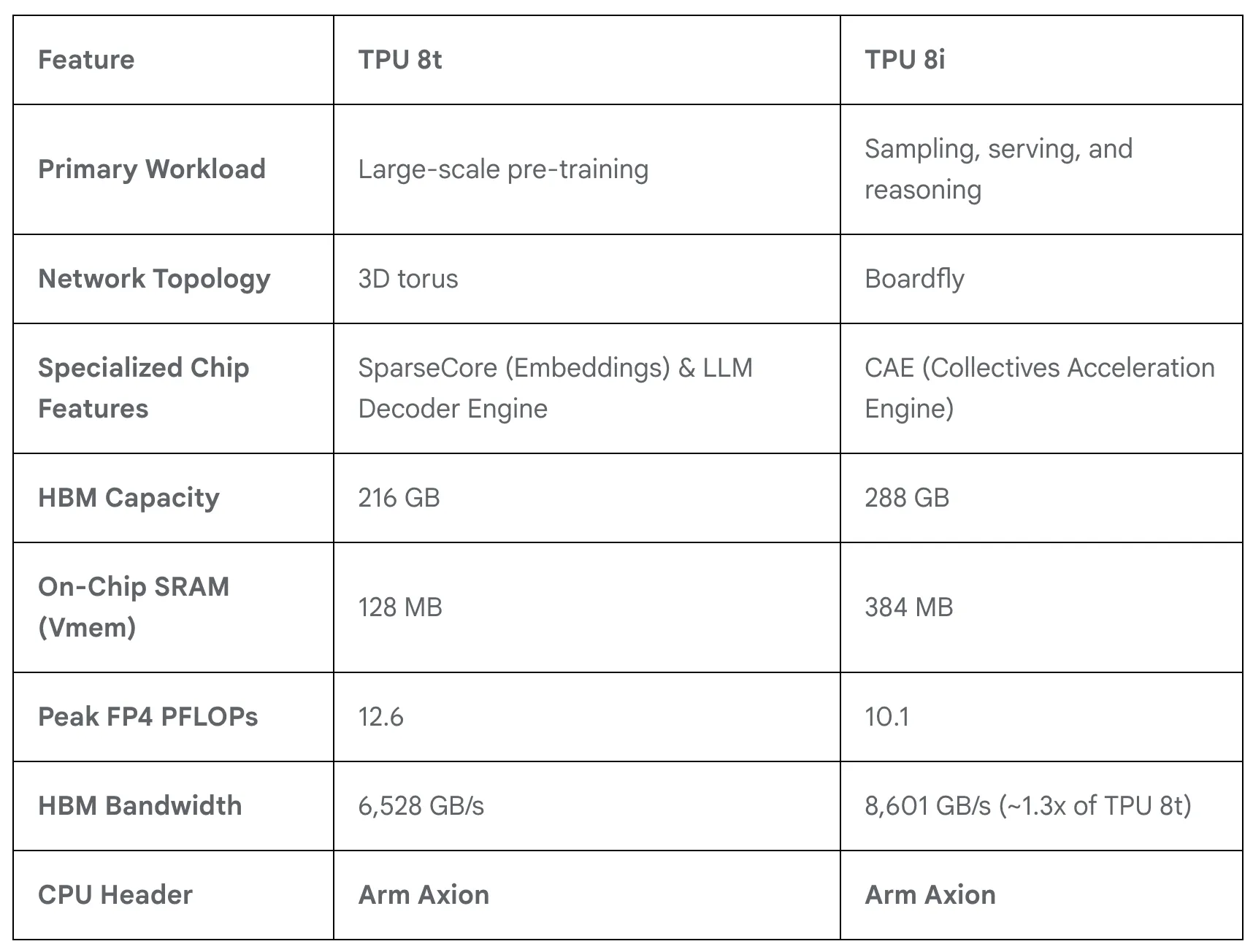
Feature-level comparison of the 8t and 8i. From the Google Cloud technical deep dive.
To understand why this is such a big deal, we first need to understand how these two different workloads compare, and why the network is the real bottleneck.
(Note: It’s worth noting that GPUs are general-purpose parallel processors, whereas TPUs are Application-Specific Integrated Circuits (ASICs). Because Google builds TPUs exclusively for AI workloads, they can strip out general-purpose bloat and optimize purely for them. However, for the sake of brevity, I won’t be covering this in detail here.)
Training vs. Inference Workloads
The demand profiles for training and inference are essentially inverses of each other:
- Training: Training a massive LLM doesn’t actually benefit as much from high memory capacity per chip. Instead, it is massively bottlenecked by network bandwidth and the sheer number of nodes you can string together. You need hundreds of thousands of chips passing gradients back and forth simultaneously.
- Inference: When generating tokens one by one (autoregressively) for a user, the workload is often highly sensitive to memory bandwidth and network tail latency. Cores might sit idle, waiting for the massive Key-Value (KV) cache to be loaded from memory.
Scale-Up vs. Scale-Out
When building AI supercomputers, there are two ways to connect chips:
- Scale-Up: Connecting chips together within the same local domain (like a single server rack). This connection (e.g. NVIDIA’s NVLink or Google’s ICI) is incredibly fast and essentially allows many chips to act as one giant unified GPU.
- Scale-Out: When a model is too big to fit in one rack, “scaling out” to other racks using standard networking cables (like InfiniBand or Ethernet) is typically the solution.
Cluster Strategies: NVIDIA vs. Google
For NVIDIA, their scale-up strategy revolves tightly around the rack. Their NVL72 architecture connects 72 GPUs into a single massive rack, where communication is blazing fast within the rack. But for scaling out, the moment data has to leave that rack to connect to the rest of the pod, bandwidth drops massively (at least 8x).
Why does this matter? Today’s frontier models rely heavily on Mixture of Experts (MoE). MoE requires tokens to be routed to different “experts” across the cluster, which relies on complex all-to-all communication. If your model is too big for a single rack, tokens get bottlenecked traveling across slower cables between racks.
Google takes a different approach. Because the infrastructure demands for pre-training and real-time inference have radically diverged, they engineered the 8th Gen TPUs to tackle each problem natively.
TPU 8t: The Pre-training Powerhouse
The 8t is optimized for massive-scale pre-training and embedding-heavy workloads. Arranged in a 3D torus topology, a single TPU superpod can scale up to 9,600 chips acting as one synchronous fabric using their proprietary Inter-Chip Interconnect (ICI) and Optical Circuit Switches (OCS). This translates to an absurd 121 exaflops of FP4 compute and 2 petabytes of shared HBM without hitting the same networking bottleneck.
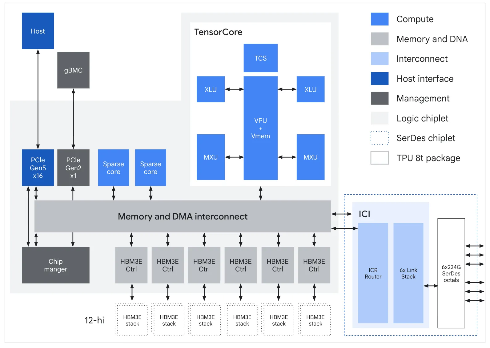
TPU 8t ASIC block diagram. From the Google Cloud technical deep dive, Figure 1.
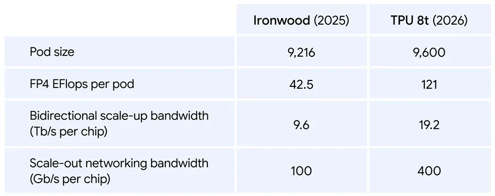
Generational jump from Ironwood (TPU 7) to TPU 8t — nearly 3x the FP4 throughput per pod and 4x the scale-out bandwidth per chip.
- The Virgo Network: Moving beyond a single 9,600-chip superpod, Google’s new Virgo network allows up to 134,000 chips to have non-blocking communication, with the ability to scale to over 1 million chips in a single training cluster with JAX and Pathways. This enables up to a 4x increase in data center network bandwidth.
- Data Ingestion: To keep these massive clusters fed, Google introduced TPUDirect Storage and Managed Lustre 10T, which bypass the CPU host entirely to route hundred-petabyte datasets directly to the silicon. Furthermore, the 8t utilizes a specialized accelerator called SparseCore to handle the irregular memory access patterns of embedding lookups, preventing the compute cores sitting idle during trillion-parameter training runs.
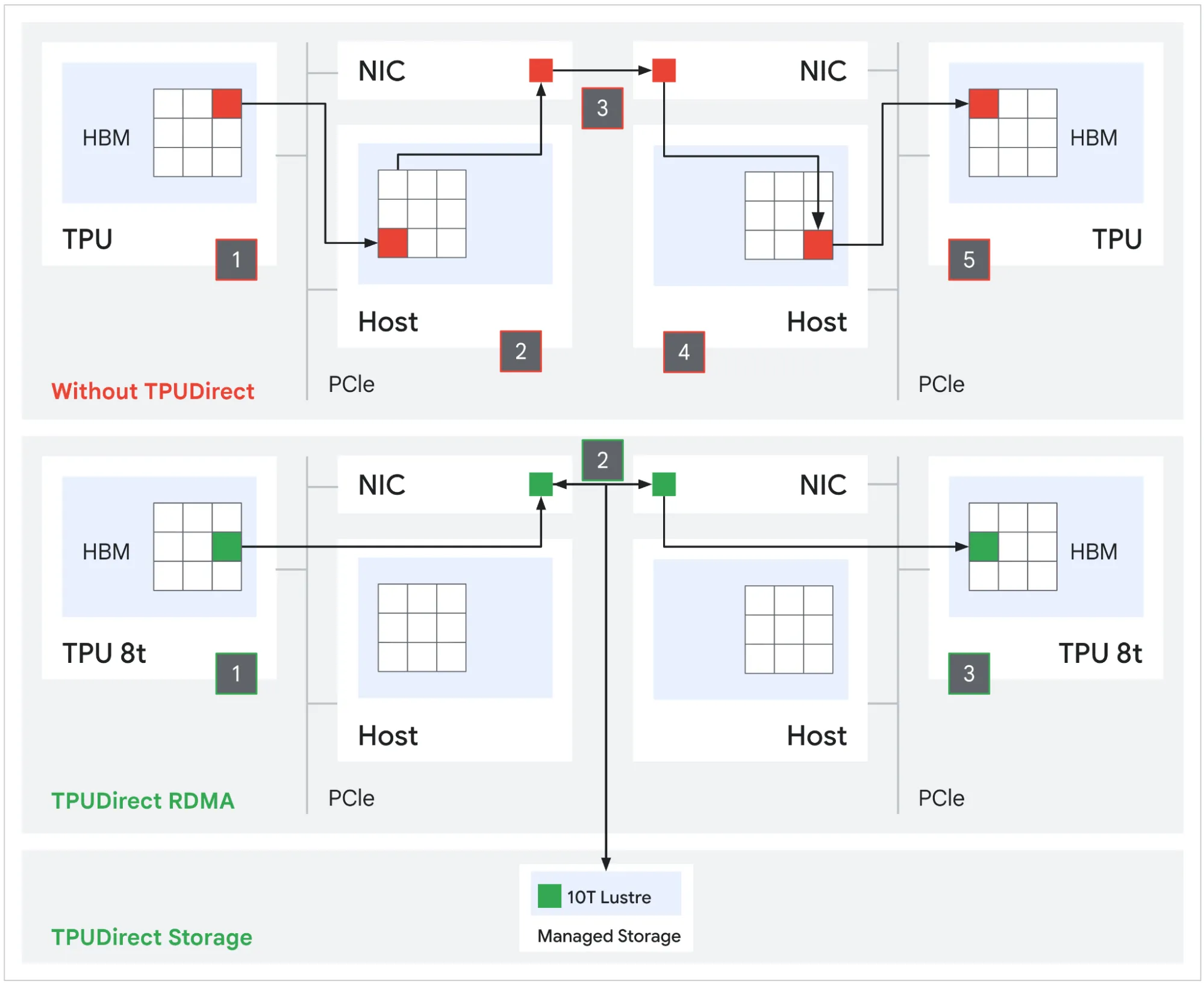
Comparison between with and without TPUDirect. From the Google Cloud technical deep dive, Figure 3.
TPU 8i: The Inference Engine
Inference for agentic AI hits what the industry calls the “latency wall”. The 8i is built specifically as a high-concurrency reasoning engine to break it.
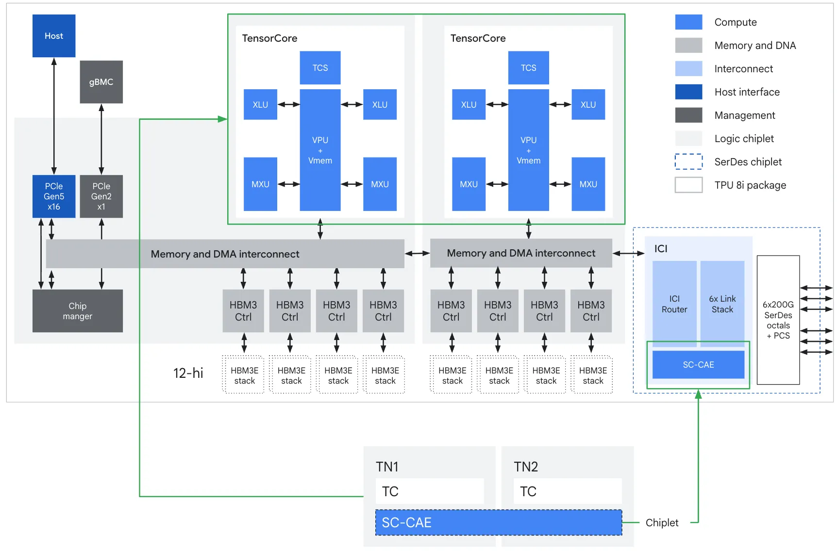
TPU 8i ASIC block diagram. From the Google Cloud technical deep dive, Figure 4.
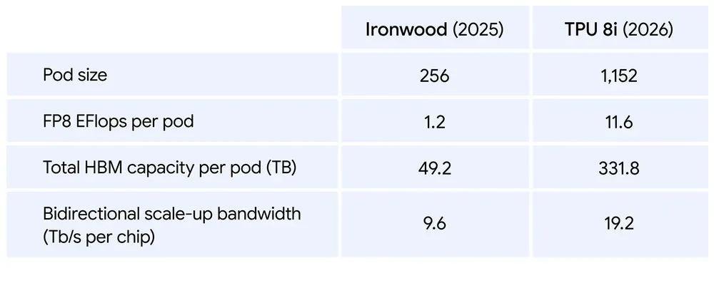
Generational jump from Ironwood (TPU 7) to TPU 8i — pod size grows 4.5x and total HBM per pod grows ~6.7x.
- Boardfly Topology: While the 8t uses a standard 3D torus mesh, the 8i introduces a hierarchical Boardfly design. By flattening the network, a TPU 8i pod (1,152 chips, up to 1,024 active) drops its maximum network diameter from 16 hops down to just 7 hops. Slashing these hops improves latency for MoE communication-intensive workloads by up to 50%.
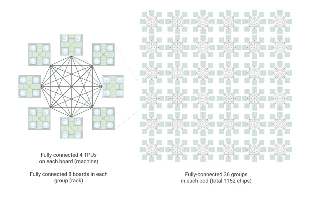
Boardfly topology with 4 TPUs per board, 8 boards per group, 36 groups per pod — 1,152 chips total, all hierarchically fully-connected.
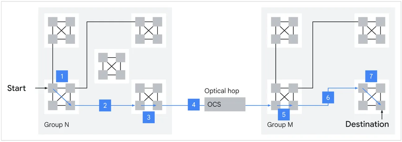
Worst-case routing across the Boardfly: 7 hops between any two chips in a pod, with one optical hop through the OCS.
- Breaking the Memory Wall: The 8i features 384 MB of on-chip SRAM (3x more than the previous generation). By keeping a larger portion of the active KV cache directly on the silicon instead of slower High Bandwidth Memory (HBM), the cores spend significantly less time idle during long-context autoregressive decoding.
- Collectives Acceleration Engine (CAE): To solve the sampling bottleneck, the 8i features a new integrated CAE that aggregates results across cores with near-zero latency. This specifically accelerates the reduction and synchronization steps required during complex “chain-of-thought” processing, reducing the on-chip latency of collectives by 5x.
If you’re interested to dive deeper, check out the following blog posts:
- Inside the eighth-generation TPU: An architecture deep dive
- Introducing Virgo Network, Google’s scale-out AI data center fabric
- Storage innovations to accelerate your AI workloads at Next ‘26
While NVIDIA dominates the per-chip specs, Google’s optical networking allows for massive scale-up domains, avoiding the severe “rack penalty” that labs might face during large-scale training and inference.
So, what does this all mean?
NVIDIA is still selling the best general-purpose AI pods to everyone, but Google’s hyper-optimized, bespoke TPU engine is proving that the winner of the AI race might just be the one who can network massive amounts of chips together with the least amount of idle time.
The ripple effects of this hardware split are massive, and I hope to dive into the economics of AI compute soon, exploring how Google’s full-stack advantage allows them to subsidize things like “AI Mode” in Search, and why Anthropic is betting billions on TPUs.
But hardware is only half the battle. I’ll also be doing a deep dive into some aspects of the software, exploring how techniques like Speculative Decoding, Multi-Token Prediction, and Quantization are breaking the memory wall from the ground up. 🙃
Other relevant links: